Magnetron sputtering (Thin Film Deposition Technique) lecture Series Part 1
1.3 هزار بار بازدید -
3 سال پیش
-
@NanotechnologyLectureSeries Sputter
@NanotechnologyLectureSeries Sputter deposition is a physical vapor deposition (PVD) method of thin film deposition by the phenomenon of sputtering. This involves ejecting material from a "target" that is a source onto a "substrate" such as a silicon wafer. Resputtering is re-emission of the deposited material during the deposition process by ion or atom bombardment. Sputtered atoms ejected from the target have a wide energy distribution, typically up to tens of eV (100,000 K). The sputtered ions (typically only a small fraction of the ejected particles are ionized — on the order of 1 percent) can ballistically fly from the target in straight lines and impact energetically on the substrates or vacuum chamber (causing resputtering). Alternatively, at higher gas pressures, the ions collide with the gas atoms that act as a moderator and move diffusively, reaching the substrates or vacuum chamber wall and condensing after undergoing a random walk. The entire range from high-energy ballistic impact to low-energy thermalized motion is accessible by changing the background gas pressure. The sputtering gas is often an inert gas such as argon. For efficient momentum transfer, the atomic weight of the sputtering gas should be close to the atomic weight of the target, so for sputtering light elements neon is preferable, while for heavy elements krypton or xenon are used.[3] Reactive gases can also be used to sputter compounds. The compound can be formed on the target surface, in-flight or on the substrate depending on the process parameters. The availability of many parameters that control sputter deposition make it a complex process, but also allow experts a large degree of control over the growth and microstructure of the film.
Uses
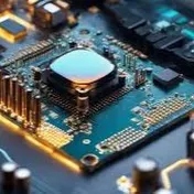
One of the earliest widespread commercial applications of sputter deposition, which is still one of its most important applications, is in the production of computer hard disks. Sputtering is used extensively in the semiconductor industry to deposit thin films of various materials in integrated circuit processing. Thin antireflection coatings on glass for optical applications are also deposited by sputtering. Because of the low substrate temperatures used, sputtering is an ideal method to deposit contact metals for thin-film transistors. Another familiar application of sputtering is low-emissivity coatings on glass, used in double-pane window assemblies. The coating is a multilayer containing silver and metal oxides such as zinc oxide, tin oxide, or titanium dioxide. A large industry has developed around tool bit coating using sputtered nitrides, such as titanium nitride, creating the familiar gold colored hard coat. Sputtering is also used as the process to deposit the metal (e.g. aluminium) layer during the fabrication of CDs and DVDs.
Hard disk surfaces use sputtered CrOx and other sputtered materials. Sputtering is one of the main processes of manufacturing optical waveguides and is another way for making efficient photovoltaic solar cells.
Sputtering sources often employ magnetrons that utilize strong electric and magnetic fields to confine charged plasma particles close to the surface of the sputter target. In a magnetic field, electrons follow helical paths around magnetic field lines, undergoing more ionizing collisions with gaseous neutrals near the target surface than would otherwise occur. (As the target material is depleted, a "racetrack" erosion profile may appear on the surface of the target.) The sputter gas is typically an inert gas such as argon. The extra argon ions created as a result of these collisions lead to a higher deposition rate. The plasma can also be sustained at a lower pressure this way. The sputtered atoms are neutrally charged and so are unaffected by the magnetic trap. Charge build-up on insulating targets can be avoided with the use of RF sputtering where the sign of the anode-cathode bias is varied at a high rate (commonly 13.56 MHz).[7] RF sputtering works well to produce highly insulating oxide films but with the added expense of RF power supplies and impedance matching networks. Stray magnetic fields leaking from ferromagnetic targets also disturb the sputtering process. Specially designed sputter guns with unusually strong permanent magnets must often be used in compensation. @Nano-Technology and Materials Science Lectures
Uses
One of the earliest widespread commercial applications of sputter deposition, which is still one of its most important applications, is in the production of computer hard disks. Sputtering is used extensively in the semiconductor industry to deposit thin films of various materials in integrated circuit processing. Thin antireflection coatings on glass for optical applications are also deposited by sputtering. Because of the low substrate temperatures used, sputtering is an ideal method to deposit contact metals for thin-film transistors. Another familiar application of sputtering is low-emissivity coatings on glass, used in double-pane window assemblies. The coating is a multilayer containing silver and metal oxides such as zinc oxide, tin oxide, or titanium dioxide. A large industry has developed around tool bit coating using sputtered nitrides, such as titanium nitride, creating the familiar gold colored hard coat. Sputtering is also used as the process to deposit the metal (e.g. aluminium) layer during the fabrication of CDs and DVDs.
Hard disk surfaces use sputtered CrOx and other sputtered materials. Sputtering is one of the main processes of manufacturing optical waveguides and is another way for making efficient photovoltaic solar cells.
Sputtering sources often employ magnetrons that utilize strong electric and magnetic fields to confine charged plasma particles close to the surface of the sputter target. In a magnetic field, electrons follow helical paths around magnetic field lines, undergoing more ionizing collisions with gaseous neutrals near the target surface than would otherwise occur. (As the target material is depleted, a "racetrack" erosion profile may appear on the surface of the target.) The sputter gas is typically an inert gas such as argon. The extra argon ions created as a result of these collisions lead to a higher deposition rate. The plasma can also be sustained at a lower pressure this way. The sputtered atoms are neutrally charged and so are unaffected by the magnetic trap. Charge build-up on insulating targets can be avoided with the use of RF sputtering where the sign of the anode-cathode bias is varied at a high rate (commonly 13.56 MHz).[7] RF sputtering works well to produce highly insulating oxide films but with the added expense of RF power supplies and impedance matching networks. Stray magnetic fields leaking from ferromagnetic targets also disturb the sputtering process. Specially designed sputter guns with unusually strong permanent magnets must often be used in compensation. @Nano-Technology and Materials Science Lectures
3 سال پیش
در تاریخ 1400/08/18 منتشر شده
است.
1,322
بـار بازدید شده